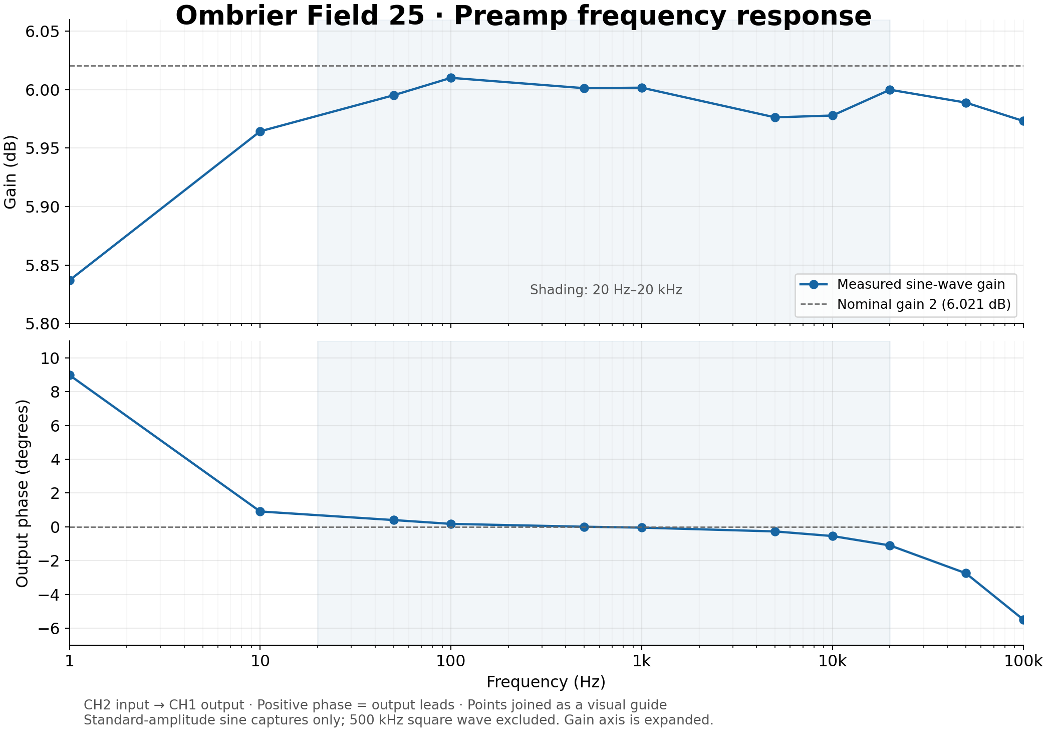
Built and measured. The first voltage-gain stage of the Field 25 amplifier, fabricated in October 2026 and measured on the bench on 4 November 2026. The gain is flat across the audio band; the distortion figure is not yet attributable to the board, and this record says so rather than printing a number it cannot defend.
Specification at a glance
| Characteristic | Verified value |
|---|---|
| Function | One channel of voltage gain ahead of the driver, direct-coupled into it |
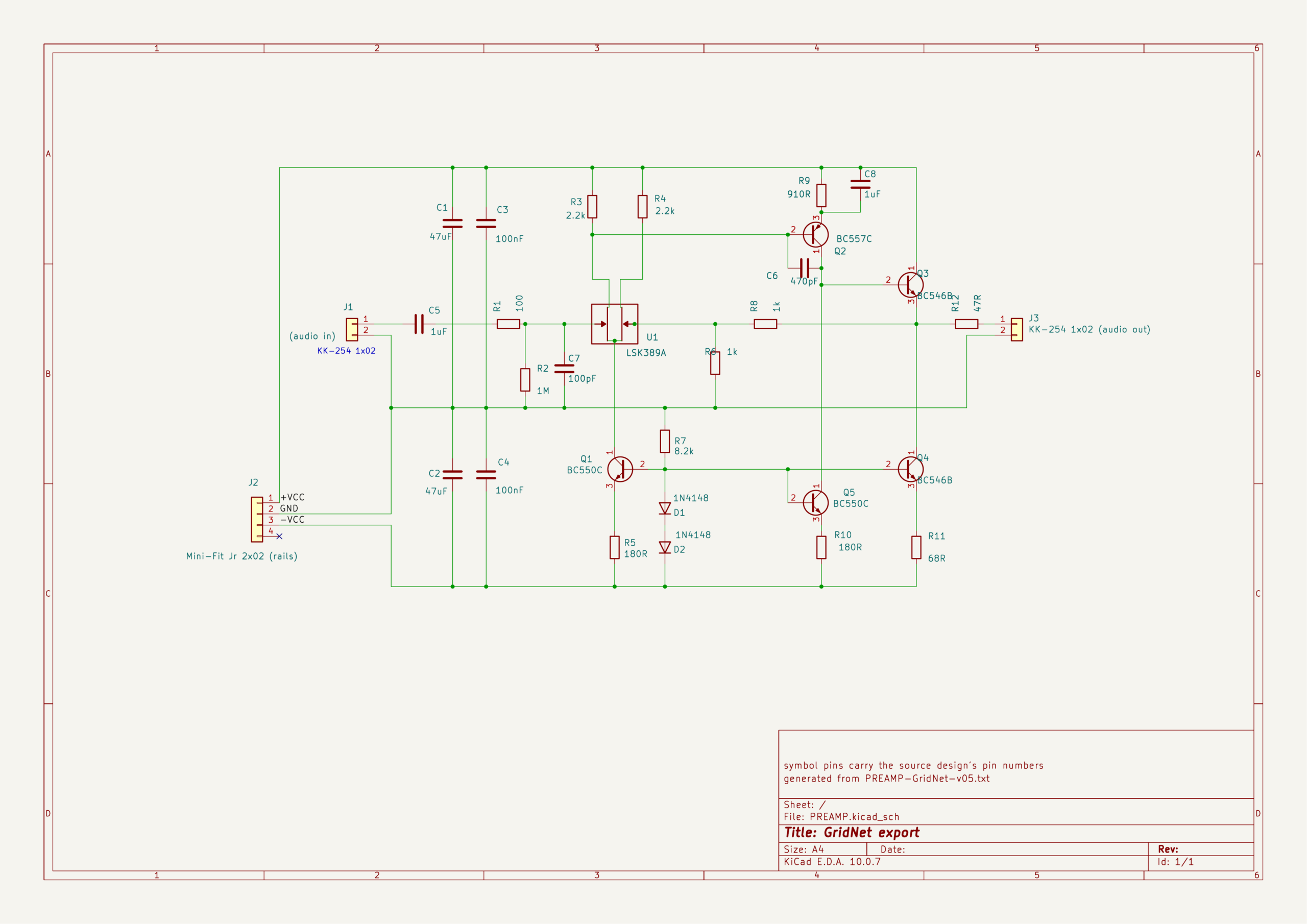
| Topology | LSK389A dual N-JFET pair at the input, BC557C level shifter, BC550C current sources, BC546B pull-down, emitter follower output through 47 Ω |
| Gain, as built | ×2 (+6,02 dB), set by R6 and R8 at 1 kΩ each; measured 1,996 V/V at 1 kHz |
| Gain flatness | 0,046 dB spread from 10 Hz to 20 kHz |
| Phase | −1,10° at 20 kHz; +8,98° at 1 Hz, the 0,16 Hz input corner of C5 1 µF with R2 1 MΩ |
| Small-signal speed | 245 ns rise and fall at a 0,203 V output step, consistent across three edges each way |
| Large-signal speed | 420 ns rise, 450 ns fall at a 2,02 V step — 3,8 V/µs |
| Distortion at 1 kHz | 0,83 % at the input, 0,86 % at the output — the preamp’s own contribution is unresolved |
| Impedances | 1 MΩ in, ≈50 Ω out; specified into the driver’s 1 MΩ, from a source of 4 kΩ or less |
| Headroom | ≈ ±27 V available (≈19 Vrms), calculated — not measured |
| Supply | ±29 V, ≈21,7 mA per rail, ≈0,6 W per board |
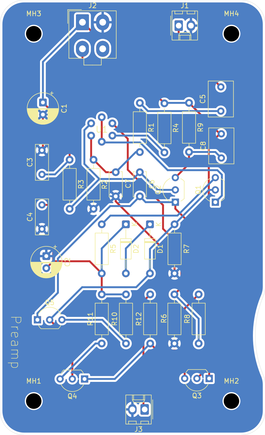
| Board | 55,0 × 90,0 mm, 2 layers, 20 nets, 73 nodes, four M3 holes at 7 mm insets |
| Revision | Schematic 26 October 2026 · bench measurement 4 November 2026 |
What it is
A differential pair of LSK389A N-JFETs at the input, a BC557C as the level shifter, two BC550C current sources and a BC546B pull-down, with the output taken from an emitter follower through 47 Ω. It behaves as a non-inverting amplifier whose feedback returns to the second gate, so the gain is set by two resistors and nothing else: G = 1 + R8/R6.
Those two resistors are a changeable element, because the gain the amplifier needs depends on the source it is fed from. Each setting lands on the same 25 W into 8 Ω at the end stage, so the board can be built for a loud 2 Vrms source or a quiet 0,5 Vrms one without touching anything else.
| Target | R6 | R8 | Gain |
|---|---|---|---|
| ×2 — as built, 2 Vrms source | 1 kΩ | 1 kΩ | 2,00 (+6,02 dB) |
| ×4 — 1 Vrms source | 1 kΩ | 3 kΩ | 4,00 (+12,04 dB) |
| ×8 — 0,5 Vrms source | 1 kΩ | 7 kΩ | 8,00 (+18,06 dB) |
The board is a closed-loop stage of its own and sits outside the amplifier’s global feedback loop: the power loop closes on the driver, not here. The 47 Ω isolation resistor is deliberately outside that loop as well, so the loop never fights this stage’s output impedance or the cable capacitance. Its linearity is therefore its own business — nothing downstream corrects it.
Schematic
Measured response
The plot at the head of this page is that sweep. It ran from 1 Hz to 100 kHz at about 0,35 Vrms in and 0,70 Vrms out. The upper −3 dB point is beyond the range of the sweep, so it is not known; 153 ns of phase lag per radian above 5 kHz is an upper bound on the stage’s own delay, because probe and channel timing were not calibrated.
What is not verified
The measurement of 4 November 2026 covers gain, phase, two step responses and harmonic content at three frequencies. It does not cover DC conditions, noise, headroom, clipping, loaded stability, the second channel, or behaviour with the driver connected. The distortion figures are the measurement chain’s, not the preamp’s: the input already carried 0,83 % at 1 kHz and more than the output at 5 kHz, so subtracting the two would be arithmetic without meaning. A fast component seen at the output connector turned out to survive shorting the probe tip to its own ground, which makes it pickup in the probe loop rather than evidence of oscillation — it does not prove the board is clean either.
Design files
The bench test report of 4 November 2026 — setup, the full sine table, both square-wave captures, the harmonic fits and the follow-up list — is available on request, as are the schematic, netlist and BOM. The engineering design record for this board is being written; until it exists, the bench report is the record.
The measurement is written up for readers rather than engineers at Two volts per volt.